English


Odisha enters global semiconductor manufacturing arena

Odisha Joins Global Semiconductor Economy with Two Major Projects
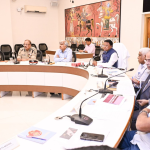
Odisha has taken a significant step into the new-age economy by entering the global semiconductor industry, particularly in the ancillary sector, Union Education Minister Dharmendra Pradhan announced on Monday.
The Union Cabinet, chaired by Prime Minister Narendra Modi, has approved the establishment of two semiconductor manufacturing units in the state. A compound semiconductor fabrication (fab) and ATMP unit will be set up in Bhubaneswar, while a 3D glass manufacturing unit will come up at Khordha’s Info Valley.
Calling it a “special gift” worth ₹2,250 crore for Odisha, Pradhan expressed gratitude to PM Modi, Chief Minister Mohan Charan Majhi, Union Electronics and IT Minister Ashwini Vaishnaw, and Odisha Electronics and IT Minister Mukesh Mahaling.
Under the India Semiconductor Mission, the Bhubaneswar facility will produce silicon carbide semiconductors used in missiles, satellites, space technology, telecom towers, and railway engines. A dedicated R&D lab will be set up at IIT Bhubaneswar, with its research park providing academic and technical support.
The Khordha unit will manufacture advanced 3D glass panels for defense, radar, aerospace, and wireless technologies. The central government will provide 50% of the funding, the Odisha government 25%, and the investor 25%. The Centre will contribute ₹700 crore for the Bhubaneswar fab and ₹800 crore for the Khordha unit, while the state will assist with land, water, electricity, and infrastructure.
Pradhan said the projects will create a semiconductor cluster in Odisha, boosting automobile and defense manufacturing, reducing import dependency, and strengthening the state’s electronics ecosystem.
Commercial production is expected within two years, generating about 1,500 direct jobs and several thousand indirect jobs.
“This marks a new chapter in the Purvoday Mission for eastern India’s development,” Pradhan said.