English
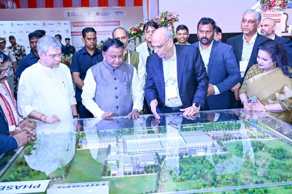

Odisha Gets India’s First 3D Chip Unit
Odisha Hosts Groundbreaking of India’s First Advanced 3D Semiconductor Packaging Unit
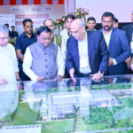
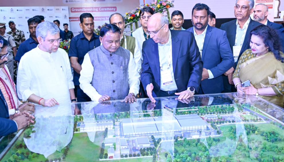
Bhubaneswar, April 19: In a landmark development for India’s semiconductor ambitions, the foundation stone for the country’s first advanced 3D semiconductor packaging unit was laid at Info Valley in Bhubaneswar on Saturday. The project is set to significantly strengthen India’s domestic electronics manufacturing ecosystem while positioning Odisha as a key technology hub.
The facility, being established by 3D Glass Solutions through its Indian arm Heterogeneous Integration Packaging Solutions Pvt. Ltd., marks a major step towards achieving the vision of Atmanirbhar Bharat in high-end electronics and semiconductor manufacturing.
The foundation stone was laid in the presence of Odisha Chief Minister Mohan Charan Majhi and Union Minister Ashwini Vaishnaw.
Describing the initiative as a historic milestone, the Chief Minister said the project brings pride to Odisha as it introduces cutting-edge 3D semiconductor packaging technology to India for the first time. He noted that global leaders such as Intel, Lockheed Martin and Applied Materials are associated with advanced packaging technologies, underlining the global relevance of the initiative.
“With this project, Odisha will play a pivotal role in realising Prime Minister Narendra Modi’s vision of a self-reliant India in semiconductor manufacturing,” he said.
The project entails an investment of nearly ₹2,000 crore and is expected to produce 70,000 glass panels annually, along with 50 million assembled units and around 13,000 advanced 3D modules. It will cater to next-generation sectors such as Artificial Intelligence, high-performance computing, defence electronics, and advanced telecommunications including 5G and 6G.
Union Minister Ashwini Vaishnaw highlighted the rapid growth of India’s electronics sector, stating that production has increased six-fold in the last 12 years. He added that India has emerged as the world’s second-largest mobile phone manufacturer and a leading exporter.
He also noted that Odisha is evolving beyond its traditional strengths in minerals and metals to become a strong player in IT, electronics, and semiconductors. The project, he said, will significantly strengthen India’s semiconductor value chain.
The facility is part of the broader India Semiconductor Mission, under which two projects have already been approved for Odisha, with more proposals under consideration.
Once operational, the unit is expected to generate substantial employment opportunities for engineers, diploma holders and ITI graduates, contributing to the state’s transition towards a technology-driven economy.
The greenfield facility will cater to high-growth sectors including data centres, AI, machine learning, automotive radar, aerospace, and photonics. Commercial production is expected to begin by August 2028, with full-scale production targeted by 2030.
With this milestone, Odisha further cements its position as one of India’s fastest-growing destinations for semiconductor and electronics manufacturing.